
EDA3.0
Verification

For most of the modern semiconductor era, the industry has operated around a powerful organizing principle:
the design flow
Architecture leads to design.
Design leads to verification.
Verification leads to tape-out.
Electronic Design Automation grew up around this structure. Over decades, an extraordinary ecosystem of tools, methodologies, and engineering practices emerged to support it. Entire engineering organizations mirror the same flow — architecture teams, design teams, verification teams, validation teams. It worked remarkably well. But the era we are entering now is beginning to stress that model in ways that are becoming increasingly visible. AI is not simply another workload running on silicon. It is reshaping how silicon is designed, validated, and deployed. And in the process, it is exposing something fundamental:
The traditional design flow was never designed to manage system-level complexity across the full lifecycle of AI silicon
Over the past few years, we have had hundreds of conversations with engineers and leaders across the semiconductor ecosystem. One pattern comes up repeatedly. Engineering organizations accumulate enormous infrastructure around design and validation over decades of successful chip programs — tools, simulation environments, verification suites, and methodologies layered on top of one another across generations of silicon. Very little of that infrastructure ever disappears.
Tests are rarely retired.
Flows rarely get simplified.
The safest path is almost always to build on top of the last successful program.
This approach made perfect sense when architectures evolved incrementally from one generation to the next. But AI-era silicon introduces something different: rapidly evolving workloads, heterogeneous compute architectures, advanced packaging, and increasingly complex deployment environments. In this new world, simply adding another layer to the existing stack does not always produce better outcomes. It often adds complexity without clarity.
The industry has historically thought in terms of design flows. But AI is forcing semiconductor organizations to think in terms of something broader:
an integrated engineering stack.
Instead of isolated phases of development, the modern semiconductor lifecycle increasingly looks like this:
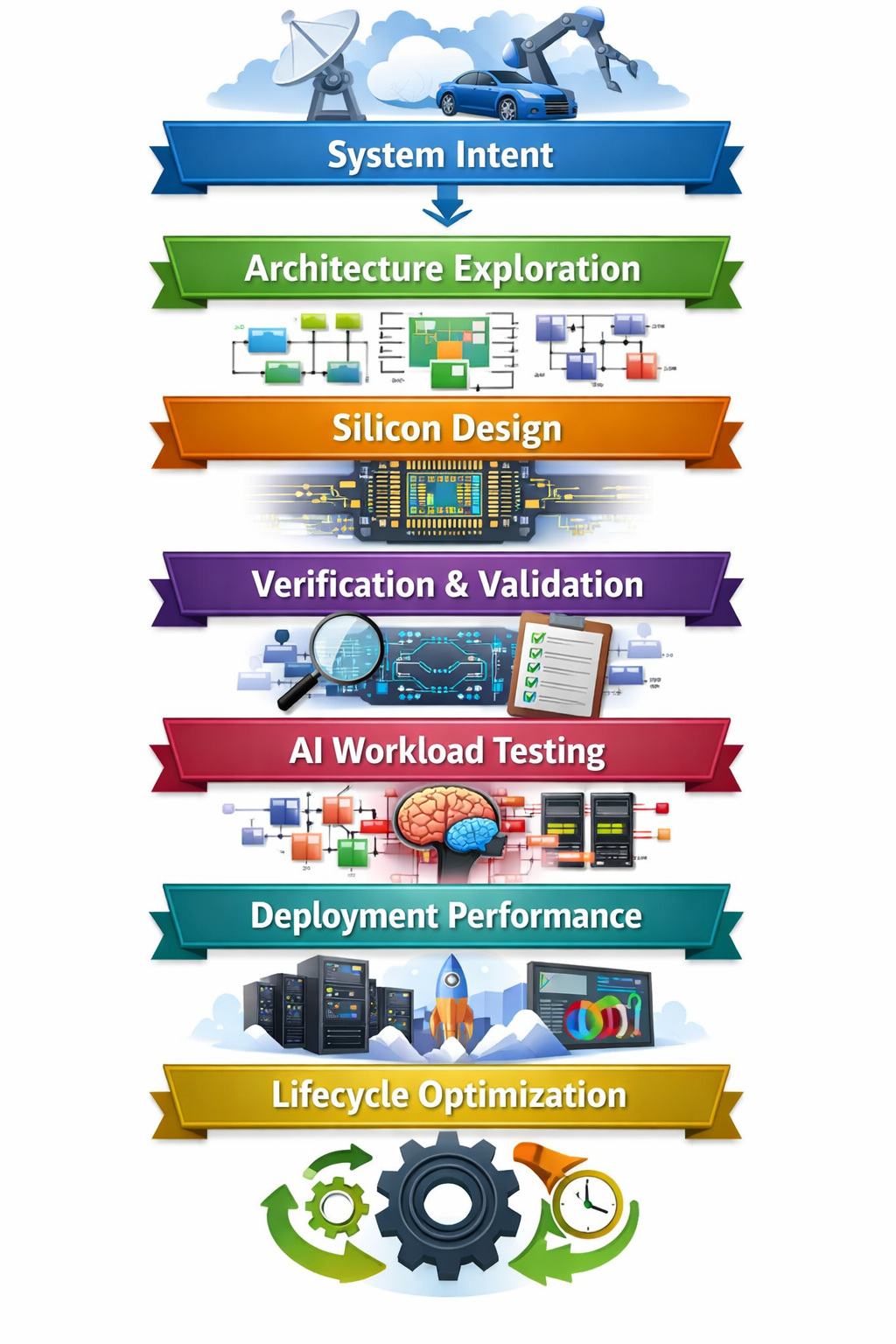
In this model, success is no longer determined solely by how efficiently a chip can be designed. Success depends on how effectively the entire engineering system connects these layers together. In other words, the challenge shifts from design optimization to systems integration across the engineering lifecycle.
The tools and organizations that power the semiconductor industry today were built to optimize individual development phases. And they have done that extraordinarily well. But optimizing each step independently does not always produce the best outcome for the system as a whole. Engineering organizations increasingly find themselves navigating questions such as:
These are not purely design-flow questions. They are engineering-stack questions.
As this shift unfolds, a new generation of companies is emerging across the semiconductor ecosystem. They do not replace traditional EDA infrastructure. Instead, they operate around the design flow, connecting the layers that historically sat outside its scope. Some focus on system-level architecture modeling. Others focus on validating silicon designs against real AI workloads before hardware exists. Still others focus on large-scale simulation environments or lifecycle optimization once silicon reaches production systems. Individually, these companies address specific problems. Collectively, they point toward something larger:
a new layer of infrastructure emerging around the semiconductor engineering stack
For engineering teams, these developments appear as new tools and methodologies. For semiconductor executives, the implications are broader. The companies that lead the AI silicon era will not simply design better chips.
They will operate better engineering systems.
They will align architecture decisions with workloads earlier. They will validate system behavior before tape-out. They will shorten the feedback loop between silicon design and real-world performance. This requires rethinking how the engineering stack itself is organized.
Between John and me, we have spent decades working across the semiconductor ecosystem — in design organizations, within EDA companies, and alongside emerging platform companies building the next generation of engineering infrastructure. We have both seen the industry evolve through several waves of abstraction and innovation. What we are beginning to see now feels like the early stages of another transition. Not a rejection of the tools and companies that built the modern semiconductor industry. But a new layer of infrastructure is needed to support the next era of silicon systems. From the Watchtower, the shift is becoming increasingly clear. The semiconductor industry is beginning to move beyond the traditional design flow toward a broader engineering stack.
And the companies that understand that transition early will shape the next decade of semiconductor innovation.
In a future Watchtower piece, we’ll explore how this shift may represent the early stages of what could become the third major era of Electronic Design Automation.
Simon Bennett & John Simmons
Co-Founders
AI Tech Sales
Read more here: AI TechSales Blog AKA The Watchtower Brief
Simon Bennett and John Simmons are Co-Founders of AI Tech Sales
Together, they have spent decades working across semiconductor design organizations, EDA companies, and emerging platform startups, shaping the next generation of silicon development.
