
EDA3.0
Verification
From the watchtower, the most important patterns rarely appear as sudden disruptions. More often, they appear as a gradual shift in how engineering organizations operate. Over the past several years, semiconductor engineering has become dramatically more complex. Photonics, chiplet architectures, heterogeneous integration, and AI infrastructure have introduced new layers of interaction across the lifecycle of a device. But complexity alone is not the defining challenge. Learning speed is. The organizations that succeed in this environment will not necessarily be those with the largest engineering teams or the most advanced design tools. They will be the ones who learn from silicon faster than their competitors.
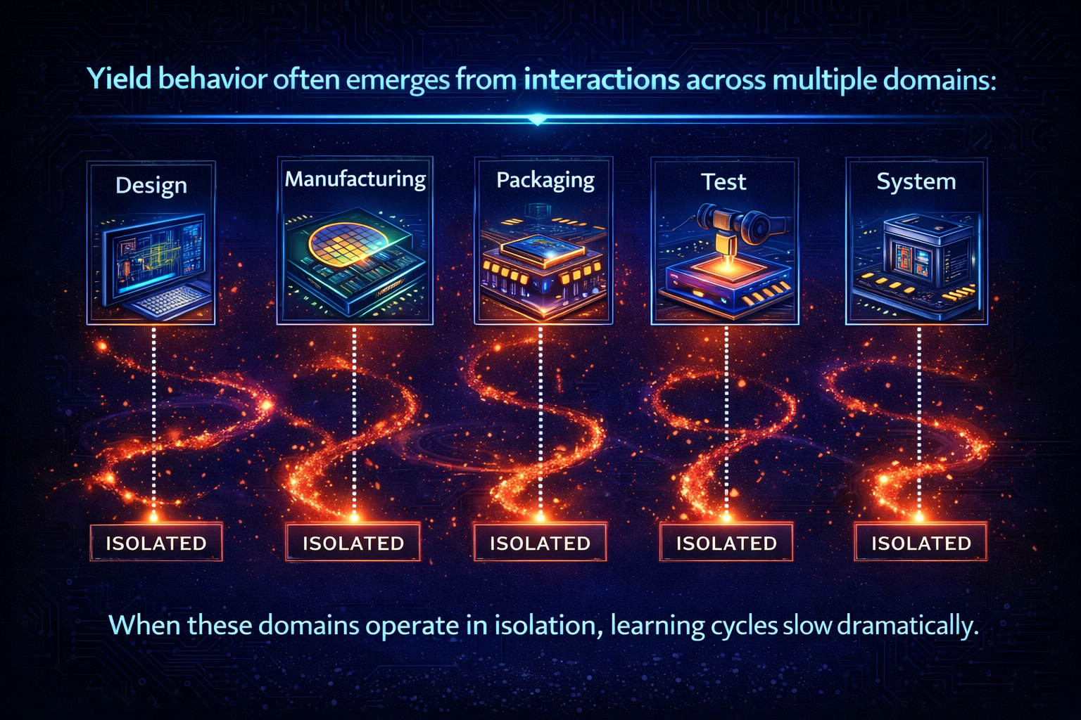
In traditional semiconductor development, yield learning followed a relatively predictable cycle. Engineers would design a device, send it through fabrication, analyze test results, and gradually improve yield through iterative design and process adjustments. This model worked well when most yield behavior could be explained by factors inside the wafer fabrication process. But the architecture of modern systems has changed. Today, yield behavior often emerges from interactions across multiple domains: Design decisions, Manufacturing processes, Packaging integration, Test environments, System-level operation. When these domains operate in isolation, learning cycles slow dramatically. Engineering teams spend weeks—or months—correlating data across systems that were never designed to work together. The problem is not a lack of data. It is a lack of connected intelligence.
Most semiconductor organizations today operate across a collection of specialized tools and systems. Design teams use engineering platforms optimized for architecture and verification. Manufacturing organizations rely on fab data systems and MES environments. Test teams maintain separate analytics pipelines. Packaging and assembly data often live in yet another ecosystem. Each system works well within its own domain. But the insights required to understand yield behavior increasingly emerge between them. When engineering teams must manually bridge those gaps, valuable time is lost. And in competitive markets, time is often the most expensive variable in the entire program.
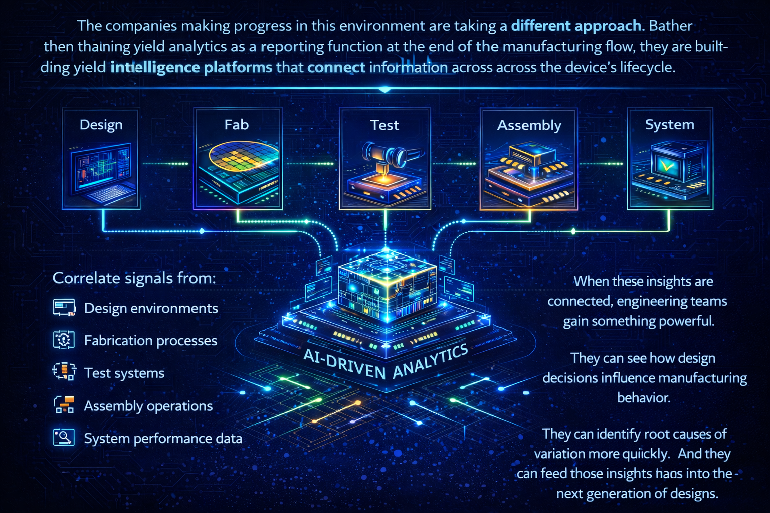
The companies making progress in this environment are taking a different approach. Rather than treating yield analytics as a reporting function at the end of the manufacturing flow, they are building yield intelligence platforms that connect information across the device's lifecycle. These platforms enable teams to correlate signals from: Design environments, Fabrication processes, Test systems, Assembly operations, and System-level performance data. When these insights are connected, engineering teams gain something powerful. They can see how design decisions influence manufacturing behavior. They can identify root causes of variation more quickly. And they can feed those insights back into the next generation of designs. In short, they learn from silicon faster.
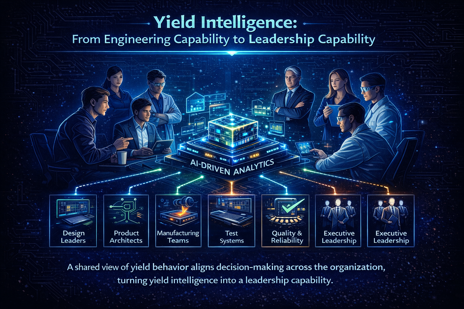
This shift is not only technical. It is organizational. In many semiconductor companies, yield management historically lived inside manufacturing operations. But as systems become more integrated, yield intelligence becomes relevant to a much broader set of stakeholders: Design leaders, Product architects, Manufacturing teams, Quality and reliability organizations, and finally, executive leadership responsible for product delivery. When these groups share a unified view of yield behavior, decision-making accelerates across the entire organization. Yield intelligence becomes not just an engineering capability, but a leadership capability.
From the watchtower, the direction is becoming clear. Photonics revealed new yield challenges. AI infrastructure is amplifying them. But the companies that succeed will not simply react to these changes. They will build systems that enable them to understand and respond faster than anyone else. The next era of semiconductor innovation will not be defined only by how quickly companies can design chips. It will also be defined by how quickly they can learn from them.
Read more articles like this one here: AI TechSales Blog AKA The Watchtower Brief
