ICTK
PUF


Two of the loudest signals in our industry right now both wear the badge of “the future.” Chiplets. Wafer-scale silicon. And both times, when I look closely, I get the same quiet feeling. I have seen this before.
That is what the Watchtower is for — watching for what is coming. Lately what is coming keeps looking a lot like what already came, and I do not mean that as a criticism. The opposite. Some of the best ideas in this business were not wrong. They were simply early. I want to tell you about two of them. One I watched as a young chip designer. One I more or less grew up on, like a lot of people who learned to love computers in Britain in the 1980s.
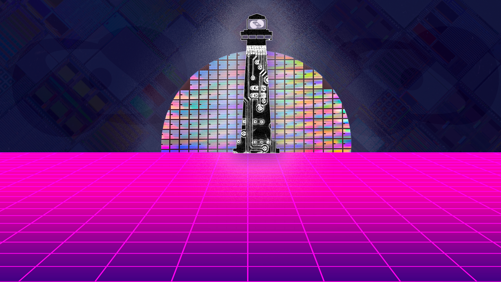
Chiplets are everywhere now. AMD, Intel, Apple, and just about every AI accelerator worth the name. The pitch is simple and good: stop trying to build one enormous chip. Build several smaller ones, each on the process that suits it, and wire them together inside a single package.
That is a multi-chip module. We had a name for it. We had several. The packaging crowd argued for years over the flavours — laminate, ceramic, and the clever one, deposited, where you lay thin-film copper and oxide straight onto a silicon substrate. IBM was shipping dozens of dies on a ceramic block in its early-1980s mainframes, the Thermal Conduction Module. The military loved MCMs because they were small and rugged. And there were startups chasing it. One I remember was nChip, doing that deposited, silicon-substrate approach. If that sounds familiar, it should. That is a silicon interposer — the heart of today's 2.5D packaging — about thirty years early. Flextronics bought nChip in 1994.
So why didn't it take over back then? Two reasons, and engineers will recognise both. The honest one is known-good die. To drop a bare die onto a module you have to be sure it is good before you commit it, because one bad die can ruin all the good ones sitting next to it — and back then, testing bare die properly was hard. The bigger reason is that Moore's Law was still cheap. Why fuss with packaging when you could wait eighteen months and get a single die that was faster and cheaper anyway? Monolithic kept winning. MCMs stayed in the niches where size and reliability paid for the trouble.
What changed is not the idea. It is the bill. Leading-edge nodes got eye-watering, the reticle puts a hard ceiling on how big one die can be, and yield punishes you for going large. The maths flipped. Around 2017 Lisa Su's team at AMD stopped treating chiplets as a packaging trick and started treating them as a strategy — compute dies on the leading node, the I/O die on a cheaper mature one, stitched together. That became Ryzen, and they out-manoeuvred a far larger rival at a fraction of the R&D. Then, in August 2022, the industry did the one thing the old MCM never managed: it agreed on a common language for dies to talk to each other, UCIe, with AMD, Arm, Intel, Qualcomm, Samsung and TSMC all at the same table.
The future arrived. It just hasn't finished arriving.
A small note of humility, because someone will spot it otherwise. The real dream of chiplets is a marketplace — mix and match the best die from anyone you like. Mostly we are not there. AMD's fabric, NVIDIA's links, Apple's package: still walled gardens. The idea is back. The open part of it is still on its way.
The second signal is louder still. Cerebras went public in May, one of the most oversubscribed listings of the year, on the strength of a chip that is, to put it plainly, the whole wafer. Most chipmakers spend their lives sawing a wafer into hundreds of small dies. Cerebras does not saw. Its Wafer-Scale Engine is a single slab of silicon about the size of a dinner plate — hundreds of thousands of cores and gigabytes of memory, all on one piece.
In their own filing they describe it as cracking a problem the industry has chewed on for roughly seventy-five years. They are right about the seventy-five years. Wafer-scale integration is old, and the reason it stayed a dream is the same word that haunted the MCM: yield. A whole wafer always has defects. You cannot make a perfect one. Gene Amdahl bet a fortune on wafer-scale with Trilogy Systems in the early 1980s, and it broke him — he reckoned a defect-free wafer was a century away.
Here is where it gets personal for those of us of a certain age and a certain passport. The man who would not let the idea die in Britain was Sir Clive Sinclair. Yes — that Sinclair. The ZX81 and the Spectrum. The little rubber-keyed machines that, for a whole generation of us who couldn't afford anything grander, were the front door into computing. I'll leave it there. You either had one, or you envied someone who did.
In 1983 Sinclair set up a research lab and advertised for people to chase the hard problems. A maverick engineer named Ivor Catt answered the advert. Catt had been patenting wafer-scale ideas since 1972 and, when the academic journals wouldn't have him, published in Wireless World in 1981. His insight is the one that still matters: stop trying to make a perfect wafer. Build in redundancy, find the good dies, and route around the bad ones. He called the routing the Catt Spiral. His own way of putting the appeal stuck with me — the wafer is a tiny fraction of the cost of the whole system, so why saw it up at all?
Sinclair backed him, bought the patents, and in 1985 spun up a company, Anamartic, with Tandem Computers among the investors. In 1989 they shipped the Wafer Stack, a wafer-scale solid-state memory, and it won product of the year — the world's first commercial wafer-scale product. Then, in 1992, it folded. Not because the idea was wrong, but because they could not get enough wafers to make it pay. The era beat the idea.
Cerebras is Catt's argument, won. The same principle — redundancy, route around the defects — now carried by 2020s process, packaging and cooling, and, crucially, a customer in AI hungry enough to pay for it. The idea was right in 1972. It just needed the world to need it.
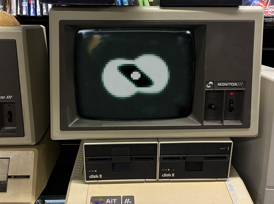
Step back and the two stories are really one story. For forty years we cut wafers into smaller and smaller pieces to dodge defects and stay under the reticle. Now we have hit a wall, and the industry has reached for two old answers at once. Chiplets say: cut it even smaller, then reconnect it properly with a standard. Wafer-scale says: don't cut it at all, build in redundancy, route around the faults. Opposite doors, the same wall.
What I take from it — and you know me, this is the optimistic bit — is that progress is not only invention. A great deal of it is an old idea meeting the moment it was waiting for. Catt, the nChip engineers, the IBM packaging people: none of them were wrong. They were early. Part of the work now is to remember them, and part of it is to be useful when their moment finally comes round.
That is the view from the Watchtower this month. The future, looking a good deal like the past, and none the worse for it.
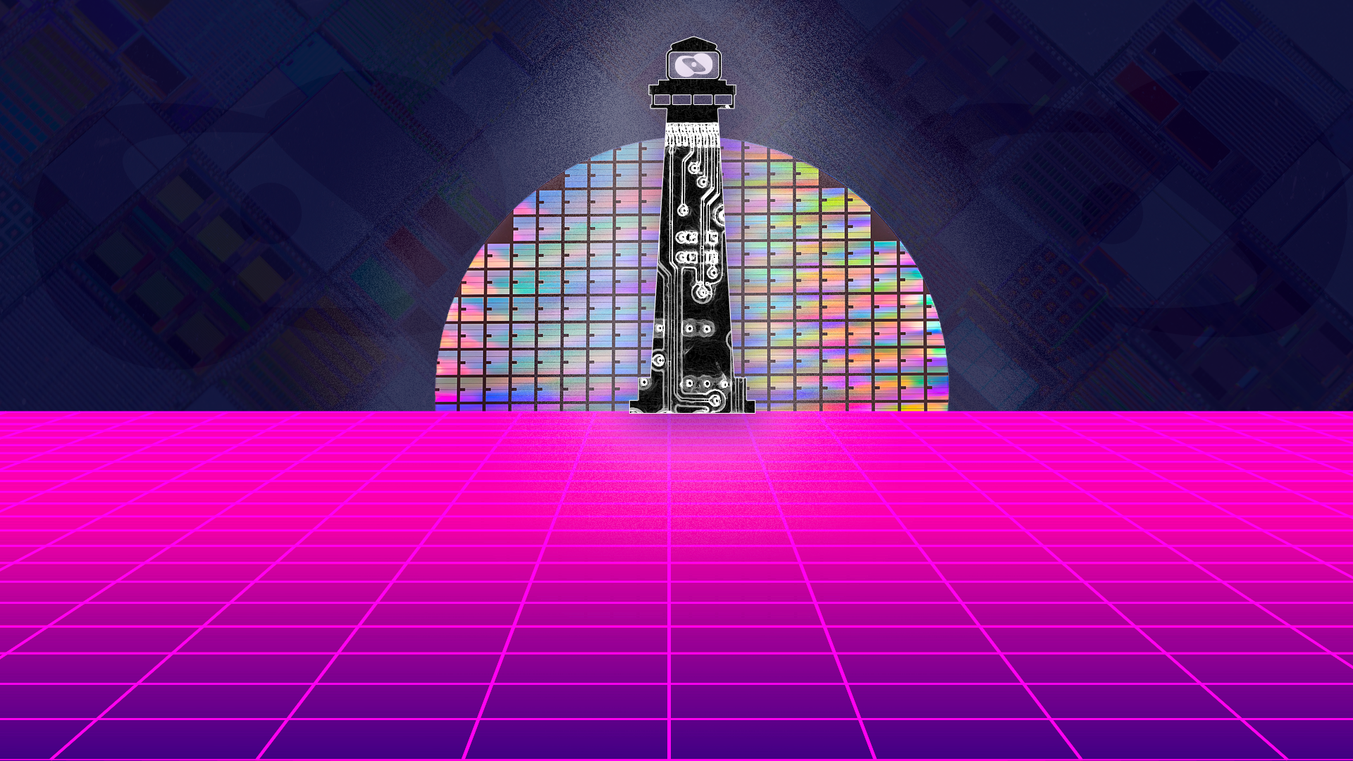
A word on the pictures. This is the first piece our Graphic Design Intern, Tony Edwards, has illustrated for us. Tony has a real feel for the retro look, and when this idea came up he was the obvious person to hand it to. A story about the past being the future deserved an artist who loves where it all came from. The good bits you see are his.
I am fairly sure I have the broad strokes right, but I watched some of this from the outside and a lot of you lived it from the inside. If you were at nChip, or you owned a Spectrum, or you remember the Wafer Stack, I would love to hear it — corrections very much included. If any of this is useful to someone a little earlier on, it was worth writing. Any thoughts greatly appreciated.
— Simon & Tony