ICTK
PUF
.png?width=1200&height=630&name=watchtower-memory-wall-social%20(2).png)

The short version: A new class of AI inference chip company is betting that memory capacity and bandwidth, not raw compute, is the real constraint on inference economics, and a growing number are placing that bet by moving away from HBM toward commodity DDR and LPDDR class memory instead. That bet quietly breaks two things at once: the UCIe chiplet IP that Synopsys and Cadence sell, which is built around a different set of packaging and memory assumptions, and the requirements traceability a fast-moving, multi-site design team needs to keep a hand-off error from turning into a re-spin. Here's why, in detail, and what's starting to fill the gap.
Look at the AI inference accelerator landscape right now and a very specific company shape keeps showing up. A small founding team, often with one foot still in a hyperscaler or an incumbent GPU vendor. A seed round that closes quietly, followed by a Series A, B, and C that arrive in tight succession rather than the usual multi-year cadence. A first product shipped in under two years. And a founding bet that sounds almost too simple to be a venture thesis: the real constraint on AI inference isn't compute, it's memory.
That bet is showing up often enough, and being financed heavily enough, that it's worth taking seriously as a category rather than a handful of unrelated startups. It's also dragging a second, less discussed bet along with it: an organizational one. That second bet is arguably the more interesting story, because almost nothing in the standard EDA or PLM toolchain was built to support it.
The memory-bound thesis has real math behind it. On a lot of the highest-value inference workloads today, long context, agentic tool use, mixture-of-experts routing, the bottleneck isn't matrix-multiply throughput, it's moving parameters and KV-cache state in and out of memory fast enough to keep the compute fed. A general-purpose GPU built to be excellent at everything ends up excellent at none of it in particular, and utilization on these workloads often lands well short of peak.
The default industry answer has been HBM: stack the DRAM vertically, put it right next to the compute die, and accept the cost. But HBM's economics have gotten genuinely brutal. Industry pricing trackers now put HBM at roughly 30 to 40 percent of total accelerator manufacturing cost, up from under 20 percent two generations ago, with HBM3E lead times sitting at 20 to 26 weeks and effectively no spot availability. Micron told investors its HBM capacity was sold out through all of calendar 2026, a sentence that reset a lot of hardware roadmaps the day it was reported.
That squeeze has opened a real strategic fork. Ride HBM's roadmap and accept the wait, the cost, and the allocation politics that come with three suppliers controlling a sold-out market. Or bet on a fundamentally different memory architecture: commodity DDR or LPDDR class memory, reached through a custom high-speed fan-out, trading peak theoretical bandwidth for capacity that HBM simply can't match per dollar or per watt.
Several of the best-funded challengers in this space have taken the second path. It's a legitimate, defensible bet. It's also one that immediately creates a physical-layer problem neither of the industry's two biggest EDA IP catalogs was built to solve, more on that below.
The technical bet rarely travels alone. Look at how these companies actually build, and a second pattern shows up just as consistently: instead of growing a large, centralized engineering organization into the complexity of the design, they run the entire flow (architecture, RTL, verification, physical design, DFT, emulation) concurrently, with a headcount that would be a single function at an incumbent, spread across a genuinely distributed set of locations. And they frequently do this while carrying a second silicon program in flight alongside the first, because the whole value proposition depends on shipping on a cadence that matches, not trails, Nvidia's own.
This isn't an accident or an early-stage growing pain. It's precisely the operating model that let a roughly 100-person team ship a first-generation product in under two years in the first place. Centralize first, then scale, and you've already lost the speed advantage that justified the company.
But it has a cost. When architecture sits in one place, verification in another, and physical design somewhere else again, and when two silicon programs are running against each other rather than in sequence, a spec change made in one location has to reach every other location's queue automatically, not because someone remembered to loop people in on Slack. Below a certain level of concurrency, that's a communication inconvenience. Above it, it's the central operational risk the company is carrying, full stop.
UCIe, Universal Chiplet Interconnect Express, was stood up in March 2022 by ten founding promoters (Intel, AMD, Arm, ASE, Google Cloud, Meta, Microsoft, Qualcomm, Samsung, and TSMC) specifically to standardize die-to-die communication so chiplets from different vendors could be mixed on one package. Both major EDA vendors have built serious, silicon-proven IP against that standard. Synopsys shipped a complete UCIe solution running up to 40 Gbps in 2024, and Cadence has progressed its UCIe PHY and controller IP through multiple tape-outs, most recently a 32G subsystem on TSMC's N3P node. This is genuinely excellent IP, and for the packaging and memory assumptions UCIe was built around, it's the right default choice for almost everyone.
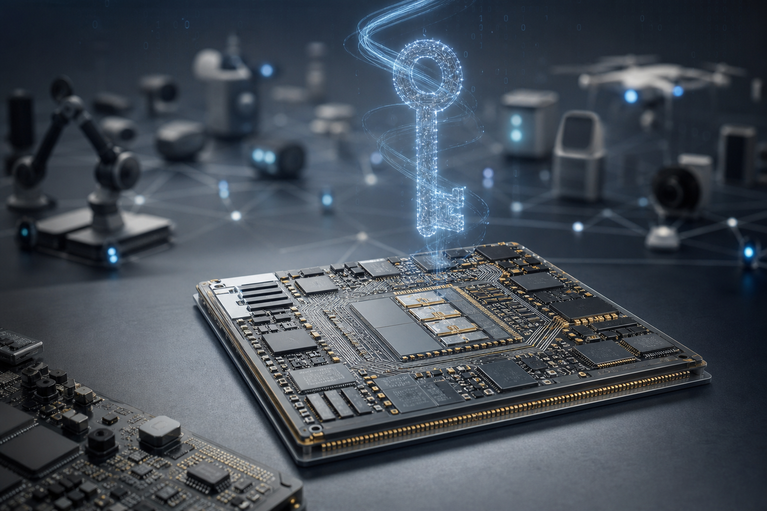
It just isn't built around a company that's deliberately walking away from HBM. Fan out a die's interface to commodity DDR or LPDDR class memory at the bandwidth these architectures need, and neither major vendor's catalog has a qualified block for the job, because that isn't the problem UCIe was standardized to solve. The result is a bespoke high-speed SerDes-to-memory-PHY interface, sourced from a specialty partner outside the two big IP houses, that then has to be verified and compliance-tested from scratch. Real, necessary engineering scope. It just lands in the gap between what Synopsys and Cadence sell and what this class of company actually needs.
Both incumbents have made real, non-trivial progress bringing AI into their own tools. Synopsys' DSO.ai uses reinforcement learning to explore floorplan and place-and-route decisions at a scale no human team could match, and has been credited with cutting a 5nm design's optimization cycle roughly tenfold. Cadence's Cerebrus Intelligent Chip Explorer and its underlying JedAI data platform do comparable work for implementation and, increasingly, specification-to-design flows built with customers like Renesas. None of that is marketing gloss. It's meaningfully faster silicon.
But every bit of it operates inside a single tool's boundary: synthesis, place and route, physical verification. None of it touches the layer sitting above the tools: whether an architectural decision made in one city is still visible, automatically, to the verification and physical-design teams working in a different one, the moment it's made, not a day later, once someone remembers to send the update.
That's a product-lifecycle-management question in every sense except the one that matters. The PLM vendors who do change-management and requirements traceability well were built for aerospace BOMs and automotive safety cases, not for a chip's V-model, its verification evidence, or its interface contracts. It falls neatly into the gap between two toolchains that were never designed to talk to each other. And that gap is exactly where a hand-off error that used to cost a team a day starts costing the company a re-spin on hardware carrying years of runway and a valuation built on hitting the next date.
This isn't a small or shrinking problem. Inference workloads now account for roughly two-thirds of all AI compute consumed, and the custom-silicon share of that compute is compounding at close to three times the rate of general-purpose GPUs. One widely cited estimate puts custom silicon at half of all AI compute capacity by 2030. Every point of that growth is another team running this exact operating model, hitting this exact gap.
Because the problem is structural (a direct consequence of how fast this category has to move, not a one-off failure of execution), the response to it has started to look structural too. Alongside Synopsys, Cadence, and Siemens, a quieter, more flexible layer of specialists has been assembling itself around exactly this gap:
None of this replaces Synopsys, Cadence, or Siemens, and it shouldn't try to. It sits alongside them, doing the connective-tissue work none of the majors have built, because it was never their job to. Call it what it actually is: an orchestration layer for the semiconductor lifecycle, running intent through yield, assembled across companies rather than owned by any single one of them. It's the layer that decides whether catching a spec change before it becomes a re-spin is a repeatable process or just a lucky week.
I've watched this exact pattern show up, account after account, often enough now that the shape is easy to recognize: fast, lean, memory-first, spread across more locations than the headcount would suggest, and one missed hand-off away from an expensive lesson on hardware that took eighteen months and nine figures to get to tape-out.
If that description lands closer to home than you'd like to admit, I'd genuinely like to hear about it. Reach out. I'll buy the coffee.
Simon Bennett
Is UCIe required for chiplet-based AI accelerators? No. UCIe is the dominant open standard and the right default for most packaging and memory choices, but it isn't mandatory. Chiplet designs built around commodity DDR or LPDDR memory instead of HBM typically need a custom SerDes-based interface that neither Synopsys's nor Cadence's UCIe catalog IP currently covers.
Why is HBM so expensive and hard to get in 2026? Industry pricing data puts HBM at 30 to 40 percent of total AI accelerator manufacturing cost, with HBM3E lead times of 20 to 26 weeks and effectively no spot market. Micron told investors its HBM capacity was sold out through all of 2026.
Do Synopsys and Cadence's AI design tools solve chip-to-chip verification or requirements tracing? No. Synopsys DSO.ai and Cadence Cerebrus and JedAI apply AI inside individual tools such as synthesis, place and route, and physical verification. None of them own the layer above the tools that traces an architecture decision through to verification evidence and physical design constraints across teams and locations.
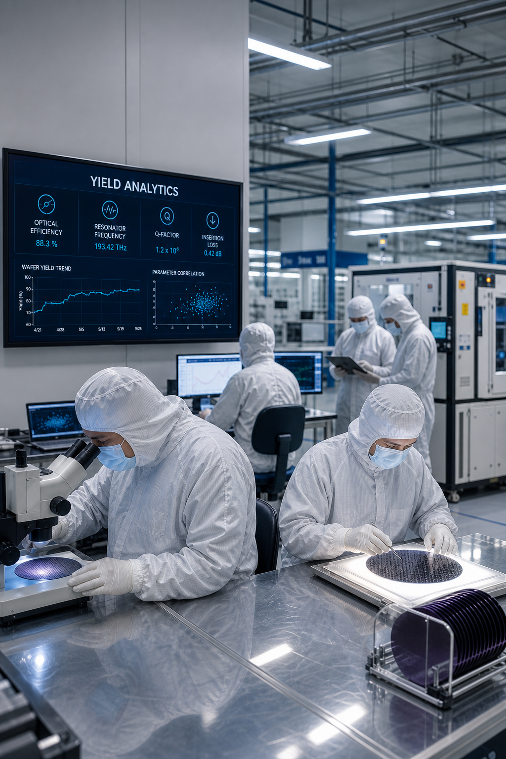
What kind of company fills the gap between EDA point tools and PLM-style requirements tracing for chips? A newer layer of specialists: die-to-die IP houses that build custom, non-UCIe chiplet interfaces, independent formal-verification practices, semiconductor-native requirements and traceability platforms, virtual-prototyping and firmware bring-up specialists for multi-die systems, and yield analytics built for first-time production ramps.
Why does a multi-site engineering team increase re-spin risk for AI chip startups? Because architecture, verification, and physical design often sit in different locations while two silicon programs run in parallel. Without an automatic way to propagate a spec change to every location's queue, a hand-off error that would normally cost a day can instead cost a full re-spin on hardware that took eighteen-plus months and nine figures to reach tape-out.