AI
EDA
EDA3.0

|
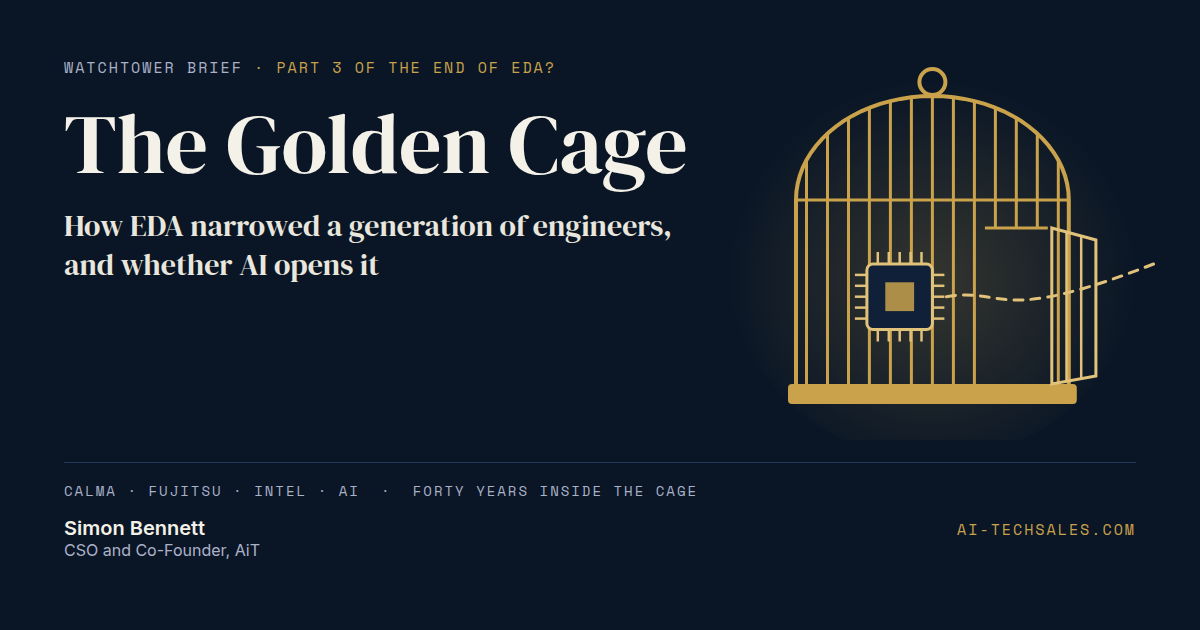
WATCHTOWER BRIEF · EDA 3.0 · AI-NATIVE DESIGN A VIEW FROM THE WATCHTOWER · PART 3 OF “THE END OF EDA?” The question is deliberately provocative. After more than forty years inside this industry, my answer is no. EDA did not take our engineers’ intelligence. We built a golden cage around where they were allowed to use it. AI can open the door, or it can gild the bars.
In The End of EDA? I argued from the top down that the intelligence in semiconductor design is moving beyond the tools. In The Problem Behind the Validation Problem I went bottom up, to the verification and validation engineers on Reddit describing narrow jobs carrying broad accountability. This third piece asks how we got here. It is the most personal of the three, because I did not read about this transition. I lived it, and in some ways I helped build it. Here is the provocation in its bluntest form: did EDA lobotomize a generation of design engineers? And if it did, is it time to claim our industry back? Where did specialization in chip design begin?For me it began at a Calma terminal. Calma’s GDS II system, introduced in 1978, was the workstation of choice for IC layout, and by the end of that decade Calma systems were installed at nearly every major semiconductor company. Its file format outlived the company by decades; we still say a design goes “from RTL to GDSII.” In my early Calma days, we did the layout of our own designs. Then something changed. We stopped doing it ourselves and started sitting next to the Calma operator, directing them verbally while they placed and routed our designs. It seemed efficient. The operator was fast at the machine, and we were free to think about the circuit. What I did not see at the time was that the work had split in two: the person who understood the design no longer touched it, and the person who touched it no longer needed to understand it. Most operators could not have cared less about the circuit. The ones who did care went on to become engineers, or applications engineers for the CAD companies. The rest disappeared along with the job.
What did the EDA playground cost us?Years later I was in Fujitsu’s ASIC division, with unlimited access to the tools from Synopsys, Cadence and Mentor (now Siemens). It was a playground. The tools were slick and polished, and they made our jobs easier. I loved it. But I noticed the team starting to specialize. I no longer had the skills to do place and route the way I had in the Calma days. I drifted toward simulation, learning Verilog and synthesis. My design partner moved toward Cadence’s Dracula, the design-rule and layout-versus-schematic checker ECAD had launched in 1983 and brought into Cadence in the 1988 merger that created the company. Nobody decided this. There was no memo. The tools drew the boundaries, each one deep enough to be a career, and the organization chart quietly followed. Job titles began to name tool stages rather than problems: synthesis engineer, physical design engineer, DV engineer, STA engineer. Each of those roles demanded real skill. That is exactly why the narrowing felt like progress. Is “lobotomy” the right word?No, and the distinction matters. The engineers I worked with did not become less intelligent. They became extraordinarily good at operating very complex systems. What changed was where their intelligence was allowed to land.
That is the golden cage. It is comfortable, well paid and full of hard problems. It rewards mastery of a complex tool rather than understanding of the whole system. And over decades it produced a kind of engineer the industry had not had before: the tool practitioner, deep in one stage of the flow, accountable for outcomes that cross every stage. That last part is the bridge to part two. When validation engineers describe narrow jobs carrying broad accountability, they are describing life inside the cage. I first used the phrase for what EDA 2.0 did to software and firmware teams in The Customer EDA Forgot. It applies to the hardware engineers too. Why did the golden cage stay closed for so long?Because the incentives on every side reinforced it. Engineering management evolved around the cage. A VP of Engineering came to be measured by how many engineers they could employ and how many licenses their organization consumed. Headcount and tool spend are visible and easy to defend in a budget meeting. Innovation produced is not. I have sat on both sides of that table, on the vendor side at Synopsys and at Intel sourcing IP from the vendors, and in The Economics of EDA I looked at how rarely anyone owns the forecast behind that spend. The vendors had their own reasons. Commercial EDA revenue scales with seats, runs and the size of the flow. An organization structured around tool boundaries is a very good customer. And then there is the human instinct every one of us has met in a senior role: five years from retirement, keep it going, vest the stock, see it through. That is not villainy. It is a rational response to the way leaders are rewarded. But it means the people with the most authority to open the cage often have the least reason to.
Is the golden cage good for the semiconductor industry?Honestly, it has been. Specialization around commercial EDA is how this industry learned to design chips with tens of billions of transistors and ship them on schedule. Without it there would be no modern SoC, no foundry ecosystem and no semiconductor IP market. The cage was golden for a reason. The cost shows up at the boundaries, and the boundaries are where today’s hardest problems live: chiplets that split a system across dies and suppliers, firmware and software that now rival the hardware effort, and silicon evidence that rarely flows back to the people who wrote the requirements. I wrote about those gaps in What Falls Between the Silos. A structure optimized for depth inside each stage struggles when the value is between them.
Can AI release engineers from the golden cage?It can, but it will not do so by default. I see two futures. In the first, AI opens the door. Agents take on the operation of the tools: setting up runs, triaging logs, chasing waivers, converting formats. Engineers get back the thing the Calma operator took from us, which is direct contact with the whole design, except now at the scale of a modern chip. One engineer can reason from intent through implementation, verification and silicon evidence again, because the machine is doing the operating rather than a person. In the second, AI gilds the bars. An agent is bolted onto each existing tool stage, priced per seat or per agent, and the organization chart does not change. The synthesis agent, the place-and-route agent and the verification agent each work faster inside the same boundaries. The practitioner is replaced, or supervised, by a practitioner model, and the system-level understanding is no more connected than before. Which future we get depends less on the technology than on two other things. How will the EDA industry protect its franchise when the value moves between the tools rather than inside them? The announcements I covered in part one suggest the incumbents are building agents into their own flows, which is sensible business and also the most natural path to the second future. And how will engineering leaders respond, particularly those whose standing rests on the size of the organization they run?
What should engineering leaders ask now?
The answer to the fifth question is the real business case for AI in semiconductor design. If the honest answer is “the same job, with fewer people,” the cage is getting smarter, not opening. What does this mean for EDA 3.0?In our EDA 3.0 framework, value is measured in outcomes such as time to market, yield and margin, not in tool speed. The organizing idea is a lifecycle where requirements, architecture, implementation, verification and silicon evidence stay connected, and where AI acts across that connection rather than inside one stage of it. That is not only a technology claim. It only works if engineering organizations and commercial models change alongside the tools. An orchestration layer laid over the same cage simply automates the cage. What evidence would settle the question?Mine is one career, and a witness is not a dataset. To test this properly I want a historical timeline of CAD and EDA set against how engineering organizations specialized; firsthand accounts from design, physical design, verification and validation engineers; a look at how engineering managers are actually measured and paid; spending and productivity measures over time; documented integration failures; and comparisons between AI-native teams and conventional ones. If you have lived any part of this, whether as an engineer who felt the walls close in, a manager who built the structure, or a vendor who sold into it, I would like to hear your story. Frequently asked questionsDid EDA make chip engineers less skilled?No. Commercial EDA made engineers highly skilled at operating complex tools, but encouraged organizations to divide work along tool boundaries. The result was deep expertise in one stage of the flow and less exposure to the system as a whole, a narrowing of scope rather than a loss of ability. What is the golden cage in semiconductor engineering?The golden cage describes a well-paid, technically demanding role defined by mastery of one stage of the EDA flow, such as synthesis, physical design or verification. It is comfortable and valuable, but it limits how far an engineer can apply their judgment across the whole design. Why did chip design teams become so specialized?As designs grew from thousands to billions of transistors, each stage of the flow became complex enough to be a career. Organizations structured teams and job titles around those tool stages, and management incentives tied to headcount and license spend reinforced the structure. What was the Calma GDS II system?Calma’s GDS II, introduced in 1978, was a minicomputer-based graphics system for IC layout that by the end of the 1970s was installed at nearly every major semiconductor company. Its GDS II stream format remains the standard for exchanging mask layout data today. Can AI reduce specialization in chip design?It can if AI agents take over tool operation and engineers are reorganized to work across intent, implementation, verification and silicon evidence. If agents are simply added to each existing tool stage, AI is more likely to reinforce today’s specialization than reduce it. Is specialization bad for the semiconductor industry?Not inherently. Specialization around commercial EDA enabled the scale of modern chip design. The cost appears at the boundaries between disciplines, such as chiplets, firmware and silicon feedback, which is where many of today’s hardest problems sit. If this matches your experience, or contradicts it, write to me directly at simon@ai-techsales.com. I am collecting firsthand accounts, and the ones that disagree with me are the most useful. Simon Bennett is CSO and Co-Founder, AiT, and founder of Kite SOC LLC. He has more than 40 years of experience in EDA and semiconductor IP, at both EDA companies and semiconductor design companies. FURTHER READING ON THE WATCHTOWER BRIEF Sources: Calma and GDS II history via the Semiconductor History Museum of Japan and EE Journal; ECAD, Dracula and the formation of Cadence via Cadence Breakfast Bytes and Encyclopedia.com. Personal recollections are the author’s own. | ||||||||||||||||