AI
EDA
EDA3.0

|
WATCHTOWER BRIEF · EDA 3.0 · AI-NATIVE DESIGN A VIEW FROM THE WATCHTOWER · OCTOBER 2026 Anthropic's S-1 is the most detailed public look yet inside a frontier AI company. It shows extraordinary demand, and an even more extraordinary bill for the silicon that serves it. That bill is about to put pressure on how chips are designed, and on how chip design is bought.
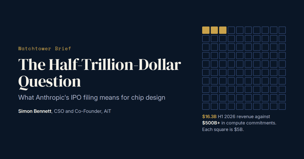
Most IPO filings put the important numbers in the income statement. For those of us in semiconductors, the most important number in this one sits in the commitments. Anthropic filed its S-1 with the SEC this morning, ahead of a planned Nasdaq listing under the ticker ANT. Most coverage will focus on valuation, governance and the size of the losses. Those are fair questions for investors. My interest is narrower: what the filing tells those of us who design, verify and sell the silicon underneath all of this. What does Anthropic's S-1 actually show?The growth is real. According to TechCrunch's read of the filing, revenue for the first half of 2026 reached $16.3 billion, up from $1.2 billion in the same period of 2025. For context, previously reported figures put full-year revenue at roughly $40 million in 2023, about $400 million in 2024 and $4.6 billion in 2025. The first half of 2026 alone is more than three times all of 2025.
Two cautions on reading those numbers. First, the net loss is not a measure of cash burn. Most of it reflects the rising value of convertible instruments, an accounting consequence of the company becoming more valuable. The operating loss is the better guide to whether the business is approaching operating leverage, and it is moving in the right direction. Second, the filing itself warns that the company may not achieve or sustain profitability. Demand at scale has been demonstrated. Attractive returns on the capital required to serve it have not yet been. Why is the compute bill the real story for chip designers?Look at where the money is committed. Reporting on the public filing lists commitments of at least $114.5 billion to Google Cloud, at least $110 billion to Amazon and at least $44.9 billion to Microsoft, plus roughly $161 billion in Broadcom leases for Google TPU hardware and further GPU capacity from neocloud providers. One early analysis of the S-1 notes the hyperscaler commitments are non-cancellable except for supplier breach. Strip away the cloud contracts and what remains is silicon: TPUs, Trainium, GPUs, HBM stacks, SerDes, optics and advanced packaging, plus the power and cooling to run them. A meaningful share of that is custom silicon designed by or for hyperscalers. The largest single line item in the most closely watched AI company in the world is, in the end, a chip bill. The same analysis reports compute and infrastructure falling from more than double revenue in early 2025 to under half of revenue by mid-2026. That trajectory is the whole investment case. It depends on revenue growing faster than compute, and every point of efficiency in the silicon helps.
A simple sensitivity makes the point. A 5% efficiency gain applied to a $500 billion spend base would be worth $25 billion. That is an illustration, not a forecast: not all of that spend is reducible and not all of it is silicon. But it explains why hyperscalers keep building their own accelerators, and why they will keep pushing their suppliers for faster design cycles. We looked at one corner of this in The Memory Wall Is Reshaping AI Inference Chip Design. Who holds the power in the AI stack?The filing describes a stack with an unusual shape. Enterprise demand flows to the model developer. The model developer depends on a handful of cloud platforms for compute. Those platforms depend on accelerator, memory, interconnect and packaging suppliers. And all of them depend on semiconductor engineering and EDA to produce the next generation of parts. What makes it unusual is that the same companies sit at several layers at once. Amazon and Google are investors, compute suppliers and distribution channels, and their cloud marketplaces carried about 47% of 2025 revenue. The S-1 itself acknowledges that these partners also build competing models. That concentration brings reach, and it brings bargaining risk in both directions. For the semiconductor industry, the practical consequence is that the buyers with the most leverage over chip roadmaps are increasingly the companies paying the compute bill, not only the companies selling chips. What does consumption pricing mean for how EDA is sold?Anthropic's revenue is overwhelmingly usage-based. Customers pay for work done, not for seats or installed capacity. Enterprise software has spent decades on the opposite model, and EDA is one of its purest examples: named licenses, token pools and multi-year subscriptions, measured largely by utilization. Once engineering teams get used to paying for AI by consumption, a different procurement question becomes natural. Not “how many simulator licenses do we need next year?” but “what does it cost to get from validated requirements to verified, manufacturable silicon?” I argued in The End of EDA? that the first commercial examples of that shift are already on the table. None of this removes deterministic verification, signoff or foundry qualification. Those stay. What may change is the interface engineers use to reach them, and the metric by which their value is judged. We explored the buyer's side of that in The Economics of EDA: Who Actually Owns the Forecast?. Is EDA being squeezed from both sides?I think there is a reasonable case that it could be, and an equally reasonable case that it will not be. Here is the first.
Traditional EDA remains indispensable in every one of those scenarios. The open question is whether it remains the dominant interface between design intent and silicon. AI could expand the semiconductor design market and, at the same time, put pressure on the licensing model that has historically dominated it. The credible alternative deserves equal weight. The incumbents have the algorithms, the installed base, the foundry relationships and the cash to integrate AI well, and they are moving quickly. If they capture the productivity gains, their franchises get stronger, not weaker. Any thesis about the future of EDA has to be tested against that outcome rather than assumed past it. Could AI agents become a new golden cage?Decades of EDA specialization rewarded tool proficiency and organizational scale. One of the more hopeful possibilities in all this is that AI returns engineers' attention to architecture, design intent and genuine invention, the work most of us came into the industry to do. But there is a new risk. If the agents orchestrating engineering work are proprietary and opaque, they can lock in customers just as effectively as any tool suite did, and with less visibility into why decisions were made. Who controls the engineering intent, the evidence and the provenance behind each decision will matter a great deal. That is the argument at the heart of What Falls Between the Silos and EDA 3.0: the value increasingly sits in the connections between requirements, architecture, implementation, verification, manufacturing and yield, and those connections should belong to the company designing the chip. That opens room for specialists: requirements and traceability, architecture exploration, virtual platforms, chiplet and packaging integration, physical IP, and manufacturing and yield analytics. Each solves a real problem. Connected through open, accountable intelligence, they can help close the gap between what a design was meant to do and what the silicon actually does. What should semiconductor leaders watch next?
I expect to come back to each of these with a longer paper. For now, my conclusion is simple. Anthropic's filing does not signal the end of EDA technology. It signals pressure on EDA's commercial and engineering model, because AI is increasing demand for specialized chips at the same time as it lowers the barriers to designing them. Both forces point the same way. This is an industry perspective, not investment advice. Figures are drawn from the public S-1 and contemporary reporting on it, and may be revised as the offering proceeds. Frequently asked questionsWhat did Anthropic's S-1 reveal about its finances?Anthropic reported $16.3 billion of revenue for the first half of 2026, up from $1.2 billion a year earlier, an operating loss of $693 million and a net loss of $80.7 billion driven largely by non-cash accounting on convertible financing. It also disclosed more than 11,900 customers spending at least $100,000 a year. Why is Anthropic's net loss so much larger than its operating loss?Most of the $80.7 billion net loss reflects non-cash revaluation of convertible financing instruments as the company's value rose. It is an accounting effect rather than cash spent on operations, which is why the $693 million operating loss is a better guide to operating performance. How much has Anthropic committed to compute infrastructure?Reporting on the S-1 puts total commitments well above half a trillion dollars over roughly a decade, including at least $114.5 billion with Google Cloud, at least $110 billion with Amazon, at least $44.9 billion with Microsoft and about $161 billion in Broadcom leases for Google TPU hardware. Why does AI's compute bill matter to chip designers?When compute is a company's largest cost, gains in silicon performance per watt and per dollar flow straight to the bottom line. That increases demand for custom accelerators, memory, interconnect and packaging, and raises the value of designing those chips faster. Will AI replace EDA tools?No. Synthesis, simulation, verification, physical design, signoff and foundry qualification remain essential. AI is more likely to change how engineers access those tools and how their value is priced, potentially shifting procurement from seats and licenses toward verified engineering outcomes. What is EDA 3.0?EDA 3.0 is AiT's term for the shift from tool-centric, siloed electronic design automation to an AI-native engineering lifecycle that connects intent and requirements through architecture, implementation, verification, manufacturing and yield, with engineering provenance carried alongside every decision. If you are working through what AI's compute economics mean for your own silicon roadmap or design flow, I would be glad to compare notes. Reach me directly at simon@ai-techsales.com. Simon Bennett is CSO and Co-Founder, AiT, and founder of Kite SOC LLC. He has more than 40 years of experience in EDA and semiconductor IP, at both EDA companies and semiconductor design companies. FURTHER READING ON THE WATCHTOWER BRIEF Sources: Anthropic, Oct 26; Anthropic S-1, SEC; TechCrunch, Oct 26; BERI; Cape Fear Advisors; Traders Union, citing Reuters; The Ringer, Sep 30. Figures as reported; the efficiency sensitivity is illustrative only. | |||||||||||||||||||||||||||