SystemVerilog
Avestra
SVA

|
WATCHTOWER BRIEF · EDA 3.0 · YIELD & MANUFACTURING AiT × YIELDWERX · A VIEW FROM THE WATCHTOWER Yield analytics grew up around CMOS logic and memory, where wafers, test programs and data formats look much the same from one fab to the next. The fastest-growing corners of the industry, from silicon photonics and MEMS to quantum devices and AR optics, look nothing like that. Their yield problems are real, expensive and arriving at volume. Their data does not fit the tools.
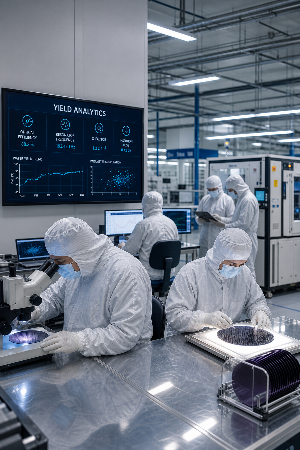
Talk to a yield engineer at a photonics or MEMS company and you will hear a familiar story told in an unfamiliar language. The wafer comes back from the foundry with a clean parametric report. Then the devices go through optical or mechanical test that the foundry never sees, then packaging, then a system-level measurement that may happen at cryogenic temperature or in a fully assembled module. Somewhere along that path, yield falls off. Finding out where, and why, usually means a person with a spreadsheet joining exports from four systems that were never designed to talk to each other. That is not a niche problem any more. Silicon photonics is moving into AI networking at volume. MEMS timing is shipping into data centres and vehicles. Photonic quantum computers are being built on commercial 300mm lines. AR waveguides are moving from prototype to supplier-scale production. Each of these markets is growing fast, and each is discovering that yield learning speed is a competitive weapon. Why do emerging technologies struggle with conventional yield tools?
What does yield look like in photonics, MEMS and optics?Silicon photonics. Photonic chips are increasingly made on standard 300mm lines, which gives them CMOS-grade wafer data. But the measurements that matter, such as waveguide loss and coupler efficiency, come from optical test that sits outside the foundry's flow. Correlating a drop in coupling efficiency with a specific process window means joining those two worlds. MEMS. A MEMS timing device combines a mechanical resonator with CMOS circuitry, made and tested separately and then packaged together. A frequency or stability excursion could start in the MEMS process, the CMOS, the package or the test itself. When a company adds an acquired product line with its own test history, the number of data sources doubles overnight. Quantum and cryogenic devices. Some of the most important measurements happen only at cryogenic temperatures, in specialised facilities, sometimes long after the wafer data was produced. Linking a cryogenic result back to a wafer lot and a process step is slow and manual in most organisations. AR optics. Waveguides patterned by nanoimprint lithography are judged on optical efficiency, uniformity and defects. As production moves to volume, often across a company site and a manufacturing partner, keeping one consistent view of yield across both becomes the difference between a profitable component and a costly one. Why not just build it in-house?Many teams do, at first. A data scientist writes scripts that pull exports together for one product. It works until the second product, the second site or the second partner arrives. Then the scripts become a maintenance burden, the original author moves on, and the organisation is back to spreadsheets during the ramp, which is exactly when it can least afford them. The other common answer is to wait for the foundry's or the test vendor's analytics to cover it. Those tools are good at what they were built for. They rarely see the optical, mechanical or cryogenic data that decides whether an emerging-technology device is good. What should yield analytics for emerging technologies do?
In our EDA 3.0 framework, this is the yield layer: the point where intent, design and manufacturing finally meet real silicon. It is also the layer the traditional design-tool incumbents have largely left alone. We made the case for closing that loop in Telemetry and EDA 3.0 and What Falls Between the Silos. How does YieldWerx approach it?YieldWerx is an established yield analytics platform built on an open, extensible architecture. It is designed to deploy quickly into brownfield environments, correlate data across domains, and sit alongside existing yield tools rather than replace them. That makes it well suited to the conditions described above: non-standard or emerging technologies, complex brownfield environments and open data.
Read more on AiT's YieldWerx page.
Frequently asked questionsWhat is yield analytics in semiconductor manufacturing?Yield analytics is the practice of collecting and correlating manufacturing and test data to find where and why devices fail, so that process, design and test can be improved. Its goal is more good devices per wafer and faster recovery from excursions. Why is yield harder to manage in photonics, MEMS and quantum devices?These technologies depend on optical, mechanical or cryogenic measurements that conventional yield tools were not designed for, their test-data standards are less mature, and the data is often split across a foundry, in-house test and partners. What is STDF and why does it matter?STDF (Standard Test Data Format) is a widely used format for semiconductor test results. It works well for conventional parametric and functional test, but many emerging-technology measurements do not fit it naturally. What is brownfield yield analytics?It means deploying yield analytics into an environment that already has manufacturing, test and analysis systems, connecting and correlating their data rather than replacing them. What is YieldWerx?YieldWerx is a yield analytics platform with an open, extensible architecture designed for rapid deployment in brownfield environments and for correlating data across domains, including non-standard data from emerging technologies. Who represents YieldWerx in North America?AiT works with YieldWerx to extend its reach with senior field presence in Silicon Valley and the Western U.S. AiT works with YieldWerx in North America. If your team is living with any of this, I would be glad to hear how it shows up on your lines and to set up a technical session with YieldWerx. Reach me directly at simon@ai-techsales.com. FURTHER READING ON THE WATCHTOWER BRIEF
Sources: YieldWerx positioning per YieldWerx. Technology descriptions are general and do not refer to any specific company's programme. AiT works with YieldWerx in North America. |
|||||||||||||||||||||||||||||||||||||