ICTK
PUF

|
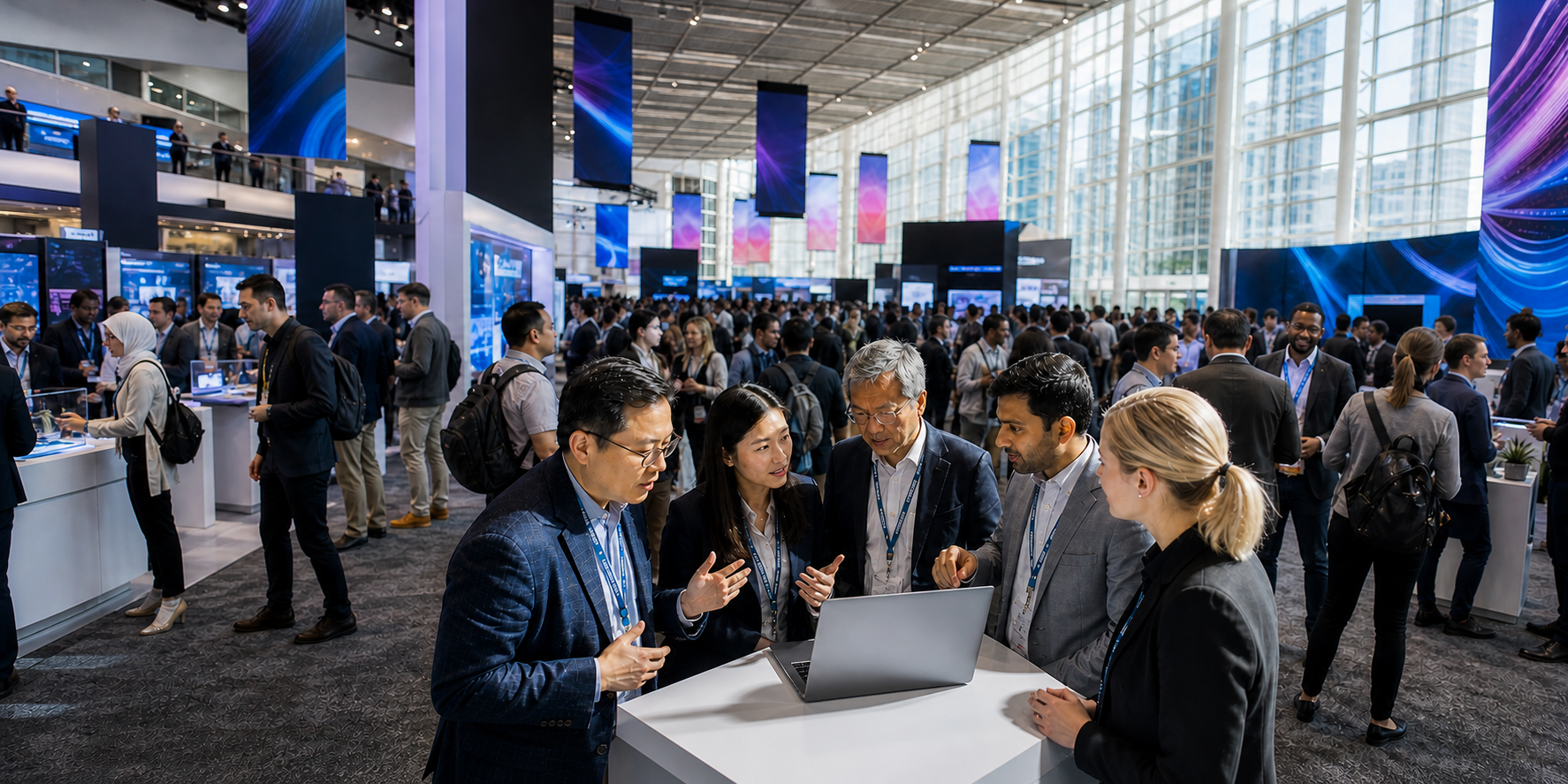
WATCHTOWER BRIEF · FIELD NOTES · SEMICON WEST 2026 A VIEW FROM THE WATCHTOWER Written on the road to SEMICON West. I left DAC impressed and a little troubled. Here's what I'm hoping a show built on manufacturing can teach an industry built on design.
The last time I walked into Moscone Center, it was for DAC, and that was a long time ago. Now I'm going back for SEMICON West, and the timing is fitting in a way I didn't plan. SEMICON West leaves San Francisco after this week and moves to an annual spring schedule at the Phoenix Convention Center beginning March 30, 2027. So I'm returning to the halls where I used to spend DAC week, this time for the manufacturing industry's flagship show, and it's the last chance to do that here. What did DAC leave me with?I came away from DAC impressed. The AI work is real. Agentic flows, assistants that actually close loops, and teams shipping instead of just demoing. There were a few real exceptions to the usual pattern too, and I wrote about one of them in The Best EDA Talk at DAC Wasn't Given by an EDA Company. I also came away troubled. I've been attending DAC for decades, and with those few exceptions its center of gravity hasn't moved. It's still about automating design in pre-silicon. The tools are faster and smarter, and AI now runs through all of them, but the conversation still mostly ends at tapeout. I made that argument in Chips to Systems, Until the System Actually Ships: the industry's idea of “end to end” stops short at both ends. Why does SEMICON have different DNA from DAC?The two shows grew from different roots. DAC started in the 1960s as a workshop where engineers automated the work of other engineers, and it became the home of EDA. Design has always been its subject. SEMICON started on the factory side. Fred Kulicke and William Hugle conceived the show in 1970, and the first one was held a year later at the San Mateo Fairgrounds, with roughly 80 exhibitors and 2,800 attendees. Over the following decade these shows helped pull a fragmented materials and equipment business into a coherent industry, and the event eventually outgrew the fairgrounds and moved to Moscone. SEMI also led the work in the 1970s on standard wafer sizes, which is a good reminder that this community has always cared about whether things fit together physically. The show stayed in the Bay Area from its start until Phoenix hosted it for the first time in 2025. So the questions are different at the root. DAC asks whether the design is correct. SEMICON asks whether it can be built, at yield, at volume and at a cost someone will pay. My bet is that the next step for our industry depends on getting those two sets of questions into the same conversation.
What actually troubles me?It's the complexity and cost of the development chain as a whole, not any single piece of it. Take any modern system, whether it's a data center rack or a robot. You need silicon, often several chiplets from several sources. You need firmware and software that has to be ready before the silicon is. You need packaging, which has become its own design and manufacturing problem. Then boards, bring-up, deployment, field failures and returns. Each stage has its own vendors, data formats, tools and geography. The number of moving parts across that chain, and the distances between them, is staggering. AI can help us sort through it. It can find the correlation between a test signature and a field return, flag the requirement that a design change just broke, and make sense of more data than any team could read. But the pieces still have to be built, brought together, shipped, integrated and tested. Atoms move more slowly than tokens. For the foreseeable future there's a human in the loop at every handoff that matters, and the handoffs are where things go wrong. I explored that gap in What Falls Between the Silos. Why are chiplets making the chain more complex?For most of my career, Moore's Law took care of a lot of problems for us. Every new node gave you more transistors, lower cost per function and better power, so the answer to most problems was to wait for the next shrink and integrate more onto one die. That's no longer true in the same way. Scaling continues, but each leading-edge node costs much more in wafers, masks and design effort, cost per transistor isn't dropping the way it used to, and the largest AI dies are already at the reticle limit. The industry's answer is to break the system apart: chiplets, mixed process nodes, advanced packaging, HBM stacks and now co-packaged optics. As I wrote in Old Is New Again, none of these ideas are new. Multi-chip modules and wafer-scale integration are forty years old. What's new is that economics finally require them. What gets less attention is what disaggregation does to the chain. A monolithic SoC had one foundry, one process and one test flow. A chiplet-based package can include logic from one foundry, I/O on an older node from another, third-party chiplet IP, memory from a separate supplier, an interposer and substrate from others, and assembly and test at an OSAT, often in several different countries before the part reaches a board. Each die has its own requirements, IP, yield data, known-good-die screening and provenance. The interfaces between them are now product-defining decisions, not internal details. When something fails in the field, tracing it back means crossing every one of those company boundaries. So chiplets fix a scaling problem by taking on a coordination problem. We moved complexity from inside the die to the spaces between dies, companies and countries.
Why does it feel like we're at a tipping point?Because four forces are hitting at once, and any one of them would be hard enough.
Together, these push in conflicting directions. Demand calls for more scale and speed. Geopolitics and provenance call for localization and proof. Complexity means more coordination across more parties. And the concentrated points of the supply chain are where all of it collides. A tipping point is when a system can't absorb more pressure in its current form and has to reorganize. That's how this feels to me. The way we've organized the development chain for the last thirty years, globally distributed, optimized for cost, with design and manufacturing in separate silos, is under more strain than it was built for. What comes next isn't settled. It could be consolidation, regionalization, new kinds of partnerships, or a digital thread strong enough to keep a distributed chain coherent. Most likely some of each. That's a big part of why I want to hear manufacturing people talk this week. Several Tuesday sessions touch these issues directly, from heterogeneous integration as the defining trait of “the system era,” to power delivery as the new ceiling for AI packages, to the geopolitics panel in the afternoon. How do we consolidate and localize without losing efficiency?Provenance is raising the stakes. In Where Trust Ends, And Assurance Begins, I looked at the NSA and JFAC guidance that sorts ASIC threats into eighteen categories covering the entire lifecycle, from requirements and EDA software through fabrication, packaging, test and delivery. The basic premise is that no single supplier, tool or facility can vouch for a modern chip end to end. That's becoming the default view for commercial programs too, not just defense ones. That leaves a hard tension. Proving provenance pushes us toward consolidating and localizing: fewer handoffs, shorter supply lines, more of the chain under one roof or one jurisdiction. But the global chain became global because it was efficient. Spreading it out made it lean and profitable. Reshoring adds cost, duplication and talent constraints right when the industry is being asked for more output. I don't think the answer is purely physical. Part of it has to be a digital thread: a living record of intent, requirements, IP, build data and test results that follows the product from spec to field, regardless of how many companies and countries it passes through. That's the core of what we call EDA 3.0. But a thread only helps if the manufacturing side is part of it. That's why I'm heading to SEMICON with questions instead of answers. Which Tuesday sessions am I watching?Tuesday's program has a lot that speaks directly to these questions:
What am I hoping to bring back?I'm trying to keep an open mind. DAC showed me that being impressed and being satisfied aren't the same thing. I want to learn how manufacturing people think about the chain, connect with people working on the handoffs, and share what I find. I'll post my thoughts during Tuesday and again later in the week. If you're at Moscone, come find me. Frequently asked questionsWhat's the difference between DAC and SEMICON West?DAC centers on electronic design automation and the pre-silicon design flow. SEMICON West, run by SEMI, centers on the manufacturing supply chain: equipment, materials, fabs, packaging and test. Is SEMICON West moving out of San Francisco?Yes. The October 13 to 15, 2026 show at Moscone is the last scheduled San Francisco edition. The show moves to Phoenix on a spring schedule beginning March 30, 2027. Why do chiplets make the semiconductor supply chain more complex?Each chiplet can come from a different foundry, process node and supplier, and they're joined through interposers, substrates and assembly partners. That multiplies the companies, countries and handoffs in a single product, and every one of them has to be tracked for yield, quality and provenance. Why does provenance matter for commercial chips, not just defense?Modern chips go through many organizations, tools and countries before shipping. Counterfeiting, IP leakage and supply concentration affect every program, and customers increasingly want proof of where each part came from. Can AI fix the complexity of the semiconductor supply chain?It can help by finding patterns across design, test and field data and catching what falls between teams. But physical building, shipping, integration and test remain, with people in the loop at key handoffs. What is EDA 3.0?AiT's term for AI-native lifecycle orchestration: connecting intent and requirements through design, verification and manufacturing to yield and field data, rather than optimizing individual tools in isolation. If you're working on the handoffs between design, manufacturing and the field, I'd like to hear from you: simon@ai-techsales.com. Simon Bennett, CSO and Co-Founder, AiT FURTHER READING ON THE WATCHTOWER BRIEF Sources: SEMICON West 2026 Tuesday schedule; SEMI, “SEMICON Conceived” (chiphistory.org); KJZZ and ABC15 on the move to Phoenix; SEMI press release, Aug 27 2026. | |||||||||||||||||||||||||||