|
Watchtower Brief | Interconnect & SerDes
Your SerDes closes at 112G or 224G per lane at the pin. Then the data can spend longer crossing your own die than it spent in flight on the channel. A technical brief for SerDes and interconnect engineers on where on-die latency really goes, and what a clockless link changes.
|
The short version
On a reticle-sized AI accelerator or switch ASIC, the route from the SerDes macro at the die edge to the crossbar or memory controller can run 15 to 20 mm or more. Crossing that distance with a conventional clocked pipeline costs a clock-domain crossing at each end and a retiming stage every millimeter or two, all hung off a clock tree that is losing frequency headroom at every new node.
Delay-insensitive, clockless links remove the clock from that route entirely. The idea is thirty years old in academia. What is new is that it can now be deployed as soft IP through a standard digital flow. This brief walks through the latency budget, the published research, and how Chronos Technology implements it, so you can decide whether it belongs in your next floorplan.
|
Where does SerDes latency actually go on a large AI or switch die?
SerDes teams live and die by the link budget at the pin: insertion loss, equalization, BER, and the latency through the PMA, PCS and FEC. That work is extraordinarily well understood. What gets far less attention is what happens after the deserialized data leaves the PCS and has to reach the logic that actually uses it.
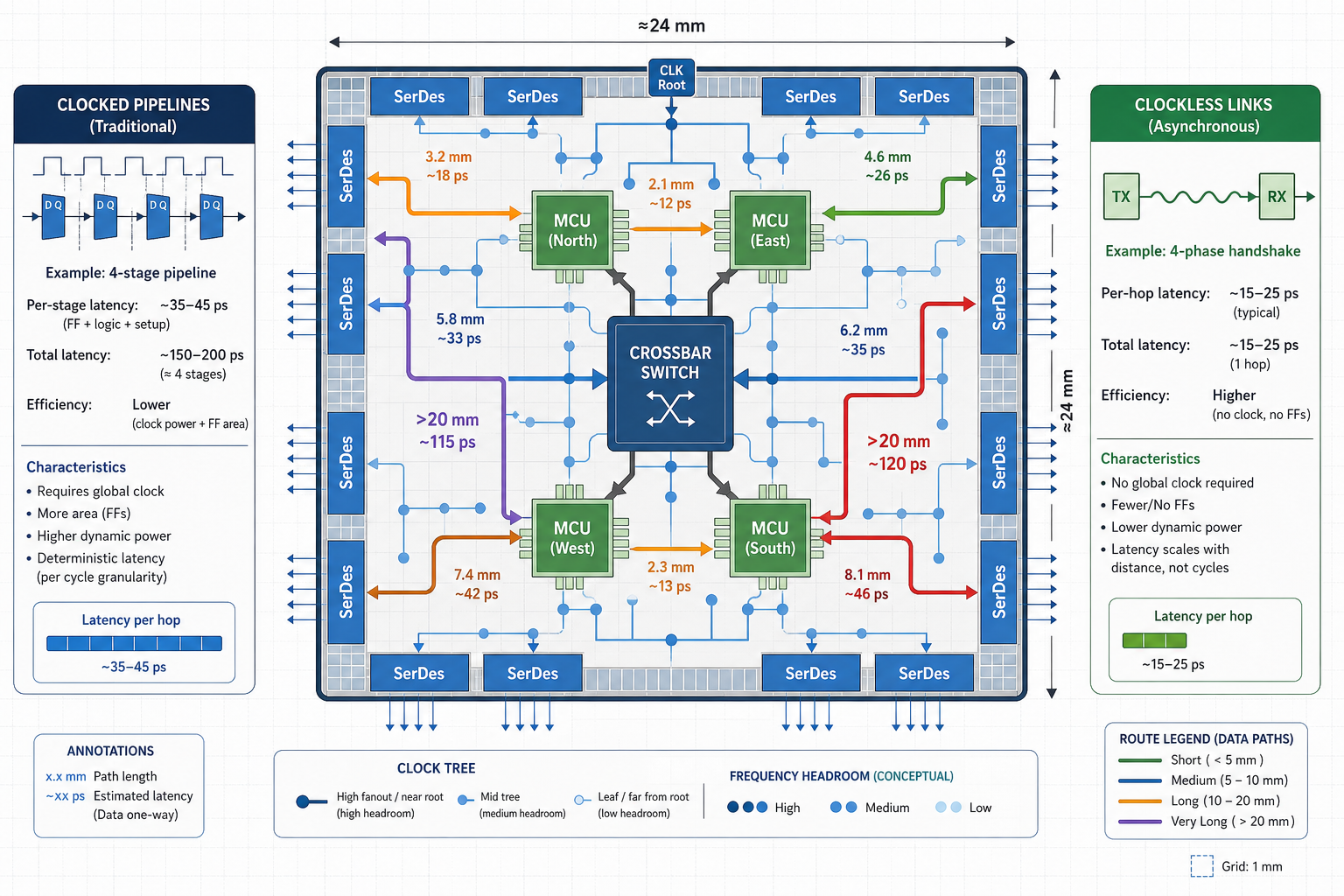
On a switch ASIC that is the crossbar. On an AI accelerator it is a NoC router, a memory controller, or a compute tile. The physical fact that makes this expensive is simple: SerDes and memory PHYs live on the beachfront, and the logic they feed lives in the middle. Chronos's own analysis of top-of-rack switch silicon notes that these dies are usually pin-limited, often reach maximum reticle size, and carry internal SerDes-to-crossbar links that can exceed 20 mm. The same geometry shows up in memory subsystems, where the distance between the system cache and the DDR PHYs at the die edge can reach 15 mm.
That distance used to be an implementation detail. It is now a first-order term in the system latency budget. Scale-up fabrics are being specified in hundreds of nanoseconds, not microseconds: OCP's scale-up Ethernet work, which Broadcom seeded with SUE and which has since grown into the ESUN workstream backed by AMD, Arista, Arm, Broadcom, Cisco, Marvell, Meta, Microsoft and NVIDIA, allocates the switch itself a budget of under 250 ns. Every nanosecond spent crossing your own die comes straight out of that allocation.
Why doesn't the clocked pipeline scale with the die?
Three things are working against the conventional approach at the same time.
Global wires stopped scaling a long time ago
Ho, Mai and Horowitz laid this out a quarter of a century ago in "The Future of Wires" (Proceedings of the IEEE, 2001): wires that shrink with the technology roughly keep pace with gate delay, but global wires that span a fixed fraction of the die do not, and their delay grows relative to the logic they connect. Die sizes have only grown since. Repeaters and pipelining hide the problem; they do not remove it.
Every retiming stage costs a clock period
The standard fix is to pipeline the route: drop a register every millimeter or two and close timing stage by stage. Each stage adds a full clock period of latency whether the data needed it or not, and each stage needs clock. Chronos puts the practical ceiling for long source-synchronous routes in current processes at under 1.5 GHz because of clock degradation, which means that even a fast core cannot run its long-haul wiring at core speed. You pay for the slowest clock you can distribute to the farthest corner of the floorplan.
Clock-domain crossings sit at both ends
The PCS runs on a clock derived from the SerDes. The crossbar runs on the core clock. Between them sits an asynchronous FIFO with a synchronizer, and on the return path another one. Each crossing costs a few cycles and a CDC sign-off item. None of it is hard; all of it is latency, area and schedule.
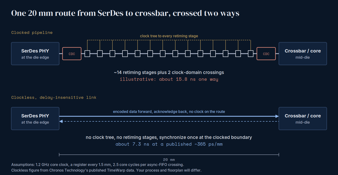
Illustrative only. The clocked case assumes a 1.2 GHz core clock, a register every 1.5 mm and 2.5 cycles per async-FIFO crossing. The clockless case uses Chronos Technology's published TimeWarp figure.
|
A back-of-envelope budget you can redo with your own numbers
| |
Clocked pipeline |
Clockless link |
| Route length |
20 mm |
20 mm |
| Retiming |
14 stages at 833 ps (1.2 GHz) |
None |
| Clock-domain crossings |
2 async FIFOs, about 2.5 cycles each |
Synchronization included in link figure |
| One-way latency |
about 11.7 + 4.2 = 15.8 ns |
20 mm × ~365 ps/mm = 7.3 ns |
A packet through a switch makes at least two of these trips, ingress SerDes to crossbar and crossbar to egress SerDes. On these assumptions that is roughly 17 ns saved per trip through the switch, or about 7 percent of a 250 ns switch budget, before counting the clock-tree power and routing you no longer need. Change the assumptions and the answer moves; the point is that the term is large enough to be worth measuring.
|
What is a delay-insensitive, clockless link?
Instead of sampling data against a clock edge, a delay-insensitive (DI) link encodes the data so that the receiver can tell from the wires alone when a complete, valid symbol has arrived, and sends an acknowledge back. Quasi-delay-insensitive (QDI) logic builds the encoders, decoders and pipeline control on the same principle. Correct operation does not depend on how long any wire or gate takes, which is exactly the property you want on a long, variable, crosstalk-prone global route.
None of this is new, and that is part of the case for it. The research record is deep:
| Work |
What it showed |
| Bainbridge & Furber, ASYNC 2001 |
A delay-insensitive SoC interconnect using 1-of-4 encoded channels, reimplementing the MARBLE bus, delivered higher throughput than a tristate bus on a narrower datapath. |
| Bainbridge & Furber, CHAIN, IEEE Micro 2002 |
A fully self-timed chip-area network that guarantees correct operation regardless of the distribution of delays in gates and wires. |
| Teifel & Manohar, ASYNC 2003 |
A clockless serial link transceiver whose token-ring architecture removes clock generation and synchronization circuitry, with a receiver that self-adjusts to the transmitter's bit rate. |
| Bainbridge, Plana & Furber, DATE 2004 |
CHAIN in a production smartcard chip: a narrow, high-frequency serial fabric with no high-frequency clock, and no timing analysis needed on the interconnect. |
| Shi, Furber, Garside & Plana, ASYNC 2009 |
SpiNNaker's system-wide DI fabric, with 3-of-6 codes on chip and 2-of-7 codes between chips, and the fault-tolerance work needed to make it robust. |
If the physics was settled twenty years ago, why is every large die still full of retiming flops? Because the research was built by asynchronous-design specialists using custom cells and custom tools. Most SerDes and SoC teams have neither, and no program manager will bet a tape-out on a methodology the team has never signed off. The blocker was never the circuit. It was the flow.
How does Chronos implement a clockless link in a standard digital flow?
That flow problem is what Chronos Technology was built to solve. The San Diego company's patent portfolio, including US 10,073,939 and US 11,205,029 on the Chronos Link protocol and US 11,418,269 on Chronos Channels, describes the approach in detail. Channels carry data using DI codes and QDI logic, which makes them insensitive to wire and gate delay variation except on a small set of isochronic forks. Their distinguishing feature is temporal compression: asynchronous serialization inside the channel, at any rational compression ratio the process can support, which is how the link narrows a wide bus without a high-speed clock.
Chronos packages this as three products built on one clockless foundation, so data can move across a long die route, through a NoC and over a 3D boundary without waiting on a clock (Chronos solutions overview):
| Product |
What it does |
| TimeWarp |
The low-latency on-die link, delivered as soft IP. Chronos publishes roughly 365 ps/mm including synchronization, no distance limitation on throughput, automated generation of netlist and constraints, low EMI and reduced crosstalk, and optional bus-width reduction. |
| Retis |
A clockless network-on-chip designed for AI workloads, related to Chronos's published work on a hybrid asynchronous NoC optimized for AI. |
| Wormhole |
A 3D-IO hard macro for hybrid-bonded die stacks: correct by construction, with no multi-die STA required, no clock crossing the bond, and pre- and post-bond test. |
The headline numbers on the Chronos site are worth checking against your own baseline: about 0.37 ns/mm latency, 5 GHz throughput, around 0.1 pJ/bit/mm, a 50 percent reduction in top-level routing measured on a large mobile SoC, and roughly 10 percent area saved on a large SoC example, mostly from routing and clock-tree removal. Chronos is also listed in the Arm partner catalog and states compatibility with AXI, ACE, CHI and TileLink.
For a SerDes team, two properties matter more than the latency figure. First, the IP goes through the synthesis, place-and-route and STA tools you already run, so adopting it does not mean retraining the team. Second, every link carries on-die telemetry that measures real per-link performance in silicon, which Chronos positions for margining, binning, DPM analysis and adaptive voltage and frequency scaling. That is the kind of post-silicon signal we argued for in Telemetry and EDA 3.0.
Does a clockless link replace my SerDes PHY?
No, and this is the question most worth getting right. Your off-package SerDes still does the hard analog work of driving a lossy channel at 112G or 224G PAM4: equalization, CDR, FEC. A clockless on-die link does not compete with that. It sits behind the PHY and replaces the clocked plumbing between the PCS and the crossbar, the memory controller or the NoC. In practice it makes a high-speed PHY more valuable, because it stops the die from giving back the latency the PHY team worked so hard to win.
The one place the roles converge is die-to-die. For short-reach links inside a package, and especially across hybrid-bonded 3D interfaces, a clockless macro like Wormhole can carry traffic without a clock crossing the boundary, which removes an entire class of multi-die timing sign-off. We covered why that packaging shift is happening now in Old Is New Again.
Where does on-die interconnect latency matter most?
Switch and scale-up fabric ASICs. Reticle-limited, SerDes-dominated floorplans with long ingress and egress routes and a switch budget measured in hundreds of nanoseconds. This is the case Chronos models most explicitly on its TimeWarp page.
Memory-first AI inference silicon. Architectures that trade HBM for large pools of DDR or LPDDR need many memory PHYs on the beachfront and a fast path from each one to the compute. We described that class of design, and why standard UCIe IP does not fit it, in The Memory Wall Is Reshaping AI Inference Chip Design. Chronos frames the same problem as shattering the memory wall.
CPU and XPU control planes. As server CPUs spend more of their silicon moving and coordinating data rather than computing on it, as we argued in Diamond Rapids: The CPU Becomes the Control Plane, mesh and CXL latency becomes a product metric. Chronos lists reduced latency in CXL expanders among its target applications.
Hybrid-bonded 3D stacks. Any design where clock distribution across the bond and multi-die STA is becoming the schedule risk.
What should a SerDes team ask before evaluating a clockless interconnect?
|
Evaluation questions worth putting to any clockless IP vendor
| Sign-off |
How are isochronic forks and relative-timing assumptions constrained and verified in my STA flow? |
| Constraints |
Are netlist and SDC generated automatically, and how do they hold up through ECOs? |
| Boundaries |
Where does synchronization happen at the clocked IP boundary, and what does that cost in cycles? |
| Test |
What is the scan and ATPG story, and how does per-link telemetry feed margining and binning? |
| Robustness |
How is glitch and crosstalk sensitivity on QDI links handled? Bainbridge and Salisbury's ASYNC 2009 work is a useful reference point. |
| Power |
What is idle power compared with a well-clock-gated synchronous baseline, not an ungated one? |
| Process |
Which nodes are silicon-proven, and what changes when I move the soft IP to the next node? |
|
If you are licensing third-party IP of any kind, our guide to managing commercial semiconductor IP covers the diligence and lifecycle questions that sit around the technical ones.
I spent enough years at Synopsys and Intel to remember when "just add another pipeline stage" was a free answer. It stopped being free somewhere around the time die sizes hit the reticle and latency budgets dropped into nanoseconds. The SerDes teams I talk to have squeezed almost everything out of the PHY. The next few nanoseconds are sitting in the wiring behind it.
If you want to walk through your own floorplan numbers, reply to this post or reach out directly, and I will set up a technical session with the Chronos engineering team.
Disclosure: Chronos Technology is an AI Tech Sales client. Performance figures cited for Chronos products are the company's published figures; the latency budget above is an illustrative calculation, not a measured result.
Related Watchtower Briefs
Quick Answers
What is the long wire problem in SoC design? It is the growing delay, power and signal-integrity cost of global on-die routes that span a large fraction of the die. Global wires do not speed up with process scaling the way gates do, so long routes need repeaters and pipeline stages that add latency, area and clock-tree power.
Why does SerDes-to-crossbar latency matter in AI switch ASICs? Reticle-sized switch dies place SerDes at the edge and the crossbar in the middle, with internal routes that can exceed 20 mm. With scale-up switch budgets specified in the low hundreds of nanoseconds, the clocked pipeline and clock-domain crossings on those routes can consume a meaningful share of the total.
What is a delay-insensitive or QDI interconnect? A link that encodes data so the receiver can detect when a complete symbol has arrived, and acknowledges it, without a clock. Correct operation does not depend on wire or gate delay, apart from a small set of isochronic forks in quasi-delay-insensitive logic.
Does a clockless on-die link replace a SerDes PHY? No. The PHY still drives the off-package channel. A clockless link replaces the clocked, pipelined route between the PHY's PCS and the logic behind it, such as a crossbar, NoC or memory controller.
Can clockless interconnect be implemented with standard EDA tools? Historically it required specialist cells and flows. Chronos Technology's TimeWarp is delivered as soft IP with automatically generated netlist and constraints, designed to run through standard synthesis, place-and-route and STA.
What latency does Chronos TimeWarp achieve? Chronos publishes roughly 365 ps/mm including synchronization, with throughput that does not degrade with distance, about 0.1 pJ/bit/mm energy and around 5 GHz throughput.
References
R. Ho, K. W. Mai, M. A. Horowitz, "The Future of Wires," Proceedings of the IEEE, 89(4), 2001
https://doi.org/10.1109/5.920580 |
W. J. Bainbridge, S. B. Furber, "Delay Insensitive System-on-Chip Interconnect using 1-of-4 Data Encoding," ASYNC 2001
https://apt.cs.manchester.ac.uk/apt/publications/papers/async01_john.php |
W. J. Bainbridge, S. B. Furber, "CHAIN: A Delay-Insensitive Chip Area Interconnect," IEEE Micro 22(5), 2002
https://apt.cs.manchester.ac.uk/publications/papers/mm_marble.php |
J. Teifel, R. Manohar, "A High-Speed Clockless Serial Link Transceiver," ASYNC 2003
https://ieeexplore.ieee.org/document/1199175/ |
W. J. Bainbridge, L. A. Plana, S. B. Furber, "The Design and Test of a Smartcard Chip Using a CHAIN Self-Timed Network-on-Chip," DATE 2004
https://apt.cs.manchester.ac.uk/publications/papers/DATE04_john.php |
Y. Shi, S. B. Furber, J. D. Garside, L. A. Plana, "Fault-Tolerant Delay-Insensitive Inter-Chip Communication," ASYNC 2009
https://apt.cs.manchester.ac.uk/apt/publications/papers/YS_ASYNC09.php |
Chronos Tech LLC, US Patent 11,418,269 (Chronos Channels)
https://image-ppubs.uspto.gov/dirsearch-public/print/downloadPdf/11418269 |
Chronos Tech LLC, US Patents 10,073,939 and 11,205,029 (Chronos Link)
https://patents.google.com/patent/US11205029 |
Chronos Technology: TimeWarp, Retis, Wormhole and the Long Wire Problem
http://www.chronostech.com/solutions |
Open Compute Project, ESUN workstream for Ethernet scale-up networking
https://convergedigest.com/ocp-launches-esun-for-ethernet-for-scale-up/ |
|